Microprocessor 8085 Notes – Architecture & Organisation, The microprocessor is an important electronic component that acts as the brain of a computer system. It performs arithmetic calculations, logical operations, and controls the working of different devices connected to the computer. A microprocessor processes data according to the instructions stored in memory and produces the required output.
Microprocessor 8085 Notes – Architecture & Organisation
What is a microprocessor?
A microprocessor is a central part of a CPU; it is also known as the brain of a computer. It is a small electronic chip that performs calculations, processes the data and controls other components in a computer.
Definition: A microprocessor is a semiconductor, multipurpose, programmable device which takes binary data as input, processes it according to the instructions stored in memory and provides an output result.
- It is a single chip.
- Perform arithmetic, logic and control operations.
- Works on binary signals.
- It is programmable, meaning it can execute multiple instructions.
Unit of Microprocessor
Microprocessors have multiple units and can do multiple works to process data and execute instructions. There are three main units in a microprocessor.

- Arithmetic and Logic Unit (ALU): It performs arithmetic operations like addition, subtraction, multiplication and division. It also does a logical operation like comparison, using ‘and’, ‘or’, and ‘not’.
- Registers: The registers are used to hold the data and instructions temporarily inside the microprocessor during the execution of the program.
- Control Unit: The control unit works like a traffic controller inside the CPU; it ensures every part of the computer works together smoothly.
Function of the Microprocessor
- It can perform addition, subtraction, multiplication and division.
- It can do comparisons like greater than, less than or equal to.
- It can transfer the data between memory, registers and input/output devices.
- It works like a manager between the processor and external devices.
Evolution of Microprocessor
There are five generations of microprocessors.

1. First Generation
The Intel 4004 was the first commercial microprocessor. It was a 4-bit microprocessor introduced in 1971. It is used in a calculator. In 1972, Intel introduced the first general-purpose 8-bit microprocessor, named the Intel 8008.
2. Second Generation
In 1974, Intel introduced the 8080 microprocessor. It is an upgraded version of the Intel 8008. In this generation the microprocessors have a CPU, ROM, RAM, clock, and I/O ports; all are in a single package which is known as a microcontroller. In 1976, the Intel 8085, an 8-bit microprocessor, was introduced.
3. Third Generation
In 1978, Intel introduced the 8086, a 16-bit microprocessor. It was an upgrade version of the 8008. The 8086 microprocessor has 64 kb of memory space and full arithmetic execution.
4. Fourth Generation
In 1981, Intel introduced the first 32-bit microprocessor, the 80386. It has a physical memory of 4 GB. In 1982, the HP-32 microprocessor was introduced late; in 1987, the Motorola 68020, a 32-bit microprocessor, was introduced.
5. Fifth Generation
In 1993, Intel introduced a 64-bit microprocessor. Intel improves the speed of the microprocessor, and the system can run new OS like Unix, Linux, etc. The speeds of the microprocessors are 66 MHz to 233 MHz. The fifth-generation microprocessor is called a Pentium processor.
Microcomputer and Microprocessor
A microcomputer is a complete computer system built around the microprocessor, which includes a microprocessor (CPU), memory (RAM/ROM), input/output ports and storage. A microprocessor is the central processing unit (CPU) on a single integrated circuit (IC).

The instruction and data are stored in memory. The instruction stored in memory is called ‘program memory’ (PM), and data is stored in another part of memory known as ‘data memory’ (DM). The control unit is just like a manager which manages all the peripheral devices connected to the computer and also reads the instructions. The processor helps to execute the instruction using the arithmetic and logic unit. The result is sent to the output device.
| Microprocessor | Microcomputer |
|---|---|
| Single chip (CPU) | Complete computer system |
| Executes instructions | Runs programs, manages data, interacts with users |
| Intel 8086 | IBM PC (1981) |
| Needs external components | Self-contained system |
Generic Microprocessor
The modern microprocessor is a generic microprocessor. A generic microprocessor is a general-purpose CPU chip designed to perform a wide range of tasks. It can handle operating systems, application programs, games, AI applications, etc.
Generic Microprocessor Diagram
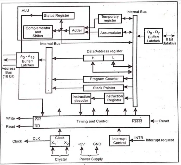
Generic Microprocessor Units
- Arithmetic and Logic Unit (ALU)
- Several registers, like the instruction register, accumulator, stack pointer, data/address register, and temporary register
- Program counter
- Instruction Decoder
- Timing and control section
- Bus buffer and latches
- Interrupt control
- Arithmetic and Logic Unit (ALU): ALUs perform the arithmetic and logical operations like addition, subtraction, multiplication and division, and the logical operations like AND, OR and NOT, etc. This result is stored in the accumulator register.
- Register: The microprocessor contains various registers. This register helps to store data temporarily during a program execution.
- Accumulator: It is an 8-bit register used to store 8-bit data. The ALU result is stored in the accumulator.
- Instruction register: It is also an 8-bit register and helps to store the first bytes of an instruction in the register.
- Status register: The status register is called ‘flags’; the status register has two flags, zero and one. These flags are made of flip-flops which have a set or reset according to data conditions in the accumulator.
- Program counter: It is a 16-bit register which contains the address of the next executable instruction.
- Stack Pointer: It is also a 16-bit register consisting of the address of a memory location called the stack.
- Data/Address Register: It is two 8-bit registers which are used separately or as a combined pair. The data are stored in this register when there is use of a pair.
- Instruction Decoder: The instruction decoder reads instructions from program memory. This instruction is a binary number. It helps to translate the binary codes into signals and tell other parts of the CPU what to do.
- Timing & Control Unit: The Timing & Control Unit is like the traffic manager inside a microprocessor. It makes sure every part of the CPU works in proper sequence and at the right time.
- Address Bus: The microprocessor uses the address bus to tell memory or input/output devices where to find or store data.
- Data Bus: The data bus is a group of 8 bits and is used for data flow between the MPU and memory and peripherals.
- Bus buffer and latches: a latch is also made up of flip-flops and stores one bit of information.
Microcomputer
A microcomputer is a complete computer system built around the microprocessor, which includes a microprocessor (CPU), memory (RAM/ROM), input/output ports and storage.
The microcomputer contain 4 blocks.
- Input Device
- Arthmetic and control unit
- Program Memory and Data memory
- Output Device
Block diagram of Microcomputer
The microcomputer is built around a microprocessor and include memory, input/output devices and storage. The block diagram shows how these components intreract.
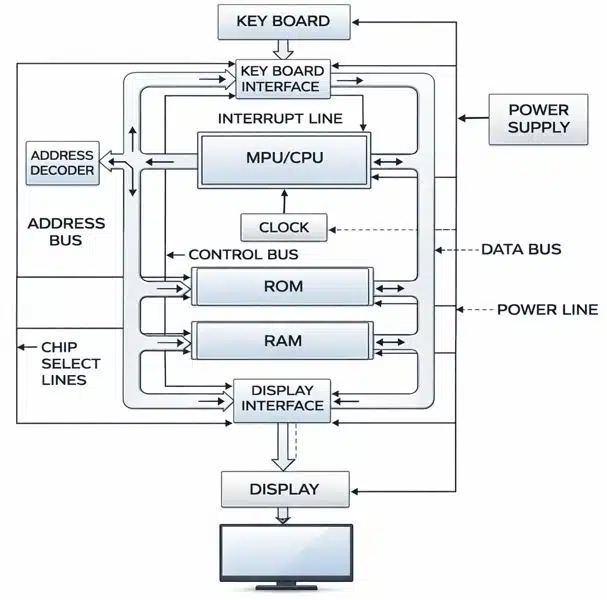
The main blocks of microprocessors are the following:
- Microprocessor (CPU): It is known as the central processing unit that executes instructions and contains the ALU, registers and control unit.
- Memory:
- RAM stands for random access memory; it is a temporary storage for data and instructions.
- ROM stands for Read-only memory; it stores permanent data for system programs.
- Input device: Takes data and instruction from the user or device, like a keyword, mouse, or scanner.
- Output device: It displays the result or processing, like a monitor, printer, or speaker.
- Storage device: It stores the data and program permanently, like a hard disc, SSD, USB drive, etc.
- System bus: There are three types of buses.
- Data Bus: It transfers data between the CPU, memory and I/O.
- Address Bus: It carries memory addresses.
- Control Bus: It helps to send control signals like read/write, clock, etc.
Block diagram of 8085
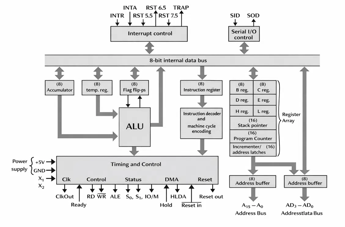
- Arithmetic and Logic Unit (ALU): It performs arithmetic and logical operations.
- Register: It is a high-speed storage location inside the CPU, like the accumulator, general-purpose registers (B, C, D, E, H, L), program counter, stack pointer, and flag register.
- Control Unit: It directly flows the data and instruction; it also controls signals for memory and I/O devices.
- Instruction Register & Decoder: It decodes the signals and tells the ALU and other units what to do.
- Timing & Control Circuitry: It manages read/write operations with memory and I/O.
- Interrupt Control: It handles external requests to pause the current program and execute urgent tasks.
- Serial I/O control: It is used for communication through SID (Serial Input Data) and SOD (Serial Output Data).
- System Bus: There are three types of buses used in the 8085.
- Address Bus: Carries memory address of 16 bit.
- Data Bus: It carries data between the CPU, memory, and I/O.
- Control Bus: It carries control signals like read, write, etc.
Features of the 8085 Microprocessor
- It is an 8-bit microprocessor, meaning it can process 8 bits of data at a time.
- It has a 16-bit address bus.
- It has an 8-bit data bus which is used to transfer data between the microprocessor and memory and I/O devices.
- It has a 3 MHz clock speed.
- It can support 74 basic instructions and 246 opcodes.
- It includes an accumulator, six general-purpose registers (B, C, D, E, H, L), a program counter (PC), a stack pointer (SP) and a flag register.
- It provides five hardware interrupts like TRAP, RST 7.5, RST 6.5, RST 5.5, and INTR.
- It has an SID (Serial Input Data) and SOD (Serial Output Data) for communication.
8085 Pin Diagram and Functions
The Intel 8085 is a 40-pin microprocessor. The pins are grouped into categories based on their function.

Address and Data Bus
- A8–A15 (Pins 21–28): Higher-order address bus (only address).
- AD0–AD7 (Pins 12–19): Multiplexed lower-order address and data bus.
Control and Status Signals
- ALE (Pin 30): Address Latch Enable – separates address from data on AD0–AD7.
- RD (Pin 32): Read signal – indicates data is to be read from memory/I/O.
- WR (Pin 31): Write signal – indicates data is to be written to memory/I/O.
- IO/M (Pin 34): Distinguishes between memory and I/O operation.
- S0, S1 (Pins 33, 35): Status signals – indicate the type of operation.
Power and Clock
- Vcc (Pin 40): a +5V power supply.
- Vss (Pin 20): Ground.
- X1, X2 (Pins 1, 2): Connected to a crystal oscillator for clock generation.
- CLK (Pin 37): Clock output for synchronising peripherals.
Interrupts and Control
- INTR (Pin 10): Interrupt request.
- INTA (Pin 11): Interrupt acknowledge.
- RST 5.5, RST 6.5, RST 7.5 (Pins 7, 8, 9): Restart interrupts.
- TRAP (Pin 6): Non-maskable interrupt.
- RST IN (Pin 36): Reset input – initialises the microprocessor.
- RST OUT (Pin 3): Reset output – indicates processor reset.
DMA (Direct Memory Access) Signals
- HOLD (Pin 39): Requests control of buses.
- HLDA (Pin 38): Hold acknowledge.
Serial I/O Ports
- SID (Pin 5): Serial input data.
- SOD (Pin 4): Serial output data.
Instruction Cycle (8085)
The instruction cycle is the sequence of operations that the 8085 performs to execute a single instruction. It consists of three main steps –
- Fetch: The microprocessor takes the instruction from memory. The program counter provides the address of the instruction, and this instruction loads on the instruction register (IR).
- Decode: The instruction decoder interprets the binary code of the instruction. It helps to identify the operation, like ‘Add’ or ‘Mov’, and the operands, registers, memory or immediate data.
- Execute: The ALU and Control Unit help to calculate the operation, and the results are stored in registers or memory; the status flags may be updated depending on the result.
Supporting Concepts
- Machine Cycle: The machine cycle is the smallest unit of the work a microprocessor does. For example, reading data from memory, writing data to memory, or reading from an input device. Each instruction is made up of one or more machine cycles.
- T-states: A T-state is just one clock pulse of the microprocessor. Every machine cycle takes a few T-states to complete.
- Instruction Cycle: An instruction cycle = Fetch + Decode + Execute. Each instruction cycle is made up of several machine cycles. Each machine cycle is further made up of several T-states.
Addressing Modes (8085)
The addressing modes tell the microprocessor how to help to find the data needed for an instruction.
- Immediate Addressing Mode – Data is given directly to the instruction, like MV1 A, 25H -> Put 25H directly into register A.
- Direct Addressing Mode – The instruction gives the memory address where the data is stored, like LDA 2050H -> Load the contents of memory location 2050H into register A.
- Register Addressing Mode – Data is inside a register. The instruction tells which register, like MOV A, B -> Copy contents of register B into A.
- Register Indirect Addressing Mode – The instruction points to a register pair (HL, BC, DE) that contains the memory address. Example: MOV A, M -> Copy data from memory location pointed to by the HL pair into A.
- Implicit (Implied) Addressing Mode – The operand is not written in the instruction; it is understood. Example: CMA. Complement the contents of the accumulator.
Disclaimer: We have provide you with the accurate handout of “Microprocessor 8085 Notes – Architecture & Organisation“. If you feel that there is any error or mistake, please contact me at anuraganand2017@gmail.com. The above study material present on our websites is for education purpose, not our copyrights.
Images and content shown above are the property of individual organisations and are used here for reference purposes only. To make it easy to understand, some of the content and images are generated by AI and cross-checked by the teachers.